- 您现在的位置:买卖IC网 > Sheet目录1194 > ADP195CP-EVALZ (Analog Devices Inc)BOARD EVAL FOR ADP195ACPZ
�� ��
��
��ADP195�
�ABSOLUTE� MAXIMUM� RATINGS�
�Data� Sheet�
�Table� 2.�
�Parameter�
�VIN,� VIN1,� VIN2� to� GND�
�VOUT,� VOUT1,� VOUT2� to� GND�
�EN� to� GND�
�Continuous� Drain� Current�
�T� A� =� 25°C�
�T� A� =� 85°C�
�Continuous� Diode� Current�
�Storage� Temperature� Range�
�Operating� Junction� Temperature� Range�
�Operating� Ambient� Temperature� Range�
�Soldering� Conditions�
�Rating�
�?0.3� V� to� +4.0� V�
�?0.3� V� to� +4.0� V�
�?0.3� V� to� +4.0� V�
�±2� A�
�±1.1� A�
�?50� mA�
�?65°C� to� +150°C�
�?40°C� to� +125°C�
�?40°C� to� +85°C�
�JEDEC� J-STD-020�
�Junction-to-ambient� thermal� resistance� (θ� JA� )� of� the� package� is�
�based� on� modeling� and� calculation� using� a� 4-layer� board.� The�
�junction-to-ambient� thermal� resistance� is� highly� dependent� on�
�the� application� and� board� layout.� In� applications� where� high�
�maximum� power� dissipation� exists,� close� attention� to� thermal�
�board� design� is� required.� The� value� of� θ� JA� may� vary,� depending� on�
�PCB� material,� layout,� and� environmental� conditions.� The� speci-�
�fied� values� of� θ� JA� are� based� on� a� 4-layer,� 4� inch� ×� 3� inch� PCB.�
�See� JESD51-7� and� JESD51-9� for� detailed� information� regarding�
�board� construction.� For� additional� information,� see� the� AN-617�
�application� note,� MicroCSP� TM� Wafer� Level� Chip� Scale� Package� .�
�Ψ� JB� is� the� junction-to-board� thermal� characterization� parameter�
�with� units� of� °C/W.� Ψ� JB� of� the� package� is� based� on� modeling� and�
�calculation� using� a� 4-layer� board.� The� JESD51-12� document,�
�Stresses� above� those� listed� under� Absolute� Maximum� Ratings�
�may� cause� permanent� damage� to� the� device.� This� is� a� stress�
�rating� only;� functional� operation� of� the� device� at� these� or� any�
�other� conditions� above� those� indicated� in� the� operational�
�section� of� this� specification� is� not� implied.� Exposure� to� absolute�
�maximum� rating� conditions� for� extended� periods� may� affect�
�device� reliability.�
�THERMAL� DATA�
�Absolute� maximum� ratings� apply� individually� only,� not� in�
�combination.� The� ADP195� can� be� damaged� when� the� junction�
�temperature� limits� are� exceeded.� Monitoring� ambient� temperature�
�does� not� guarantee� that� T� J� is� within� the� specified� temperature�
�limits.� In� applications� with� high� power� dissipation� and� poor�
�PCB� thermal� resistance,� the� maximum� ambient� temperature�
�may� need� to� be� derated.�
�In� applications� with� moderate� power� dissipation� and� low� PCB�
�thermal� resistance,� the� maximum� ambient� temperature� can�
�exceed� the� maximum� limit� as� long� as� the� junction� temperature�
�Guidelines� for� Reporting� and� Using� Electronic� Package� Thermal�
�Information� ,� states� that� thermal� characterization� parameters� are�
�not� the� same� as� thermal� resistances.� Ψ� JB� measures� the� component�
�power� flowing� through� multiple� thermal� paths� rather� than� through�
�a� single� path,� as� in� thermal� resistance� (θ� JB� ).� Therefore,� Ψ� JB� thermal�
�paths� include� convection� from� the� top� of� the� package� as� well� as�
�radiation� from� the� package,� factors� that� make� Ψ� JB� more� useful�
�in� real-world� applications.� Maximum� junction� temperature� (T� J� )�
�is� calculated� from� the� board� temperature� (T� B� )� and� the� power�
�dissipation� (P� D� )� using� the� formula�
�T� J� =� T� B� +� (� P� D� ×� Ψ� JB� )�
�See� JESD51-8,� JESD51-9,� and� JESD51-12� for� more� detailed�
�information� about� Ψ� JB� .�
�THERMAL� RESISTANCE�
�θ� JA� and� Ψ� JB� are� specified� for� the� worst-case� conditions,� that� is,� a�
�device� soldered� in� a� circuit� board� for� surface-mount� packages.�
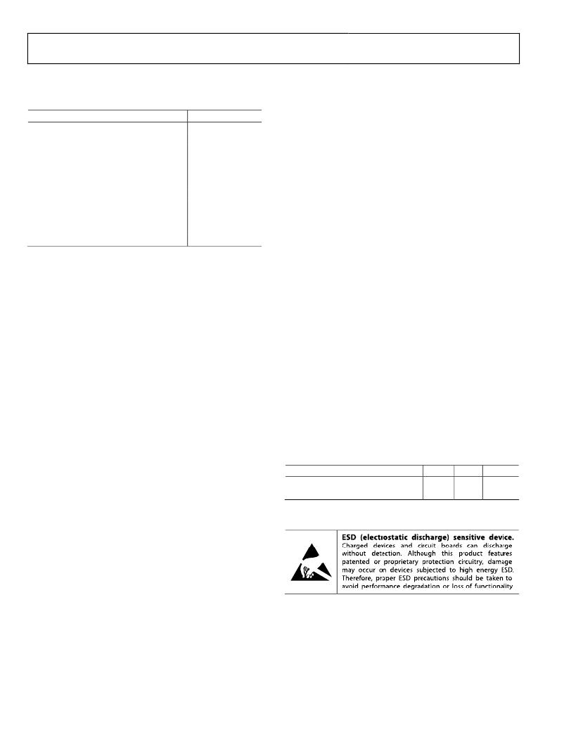
�Table� 3.� Thermal� Resistance�
�is� within� specification� limits.� The� junction� temperature� (T� J� )� of�
�the� device� is� dependent� on� the� ambient� temperature� (T� A� ),� the�
�power� dissipation� of� the� device� (P� D� ),� and� the� junction-to-ambient�
�Package� Type�
�4-Ball,� 0.5� mm� Pitch� WLCSP�
�6-Lead,� 2� mm� � 2� mm� LFCSP�
�θ� JA�
�260�
�72.1�
�Ψ� JB�
�58.4�
�24.0�
�Unit�
�°C/W�
�°C/W�
�thermal� resistance� of� the� package� (θ� JA� ).�
�Maximum� junction� temperature� (T� J� )� is� calculated� from� the�
�ambient� temperature� (T� A� )� and� power� dissipation� (P� D� )� using� the�
�ESD� CAUTION�
�formula�
�T� J� =� T� A� +� (� P� D� ×� θ� JA� )�
�Rev.� C� |� Page� 4� of� 12�
�发布紧急采购,3分钟左右您将得到回复。
相关PDF资料
ADP197CB-EVALZ
BOARD EVAL FOR ADP197ACBZ
ADP198CP-EVALZ
BOARD EVAL FOR ADP198
ADP199CB-EVALZ
BOARD EVAL FOR ADP199
ADT7462ZEVB
BOARD EVALUATION FOR ADT7462
ADT7467BBZEVB
BOARD EVALUATION FOR ADT7467
ADT7468ZEVB
BOARD EVAL FOR ADT7468
ADT7473ZEVB
BOARD EVALUATION FOR ADT7473
ADT7475EBZEVB
BOARD EVALUATION FOR ADT7475
相关代理商/技术参数
ADP195-EVALZ
功能描述:BOARD EVALUATION FOR ADP195 RoHS:是 类别:编程器,开发系统 >> 评估演示板和套件 系列:* 标准包装:1 系列:- 主要目的:电信,线路接口单元(LIU) 嵌入式:- 已用 IC / 零件:IDT82V2081 主要属性:T1/J1/E1 LIU 次要属性:- 已供物品:板,电源,线缆,CD 其它名称:82EBV2081
ADP196
制造商:AD 制造商全称:Analog Devices 功能描述:5 V, 3 A, Logic Controlled High-Side Power Switch
ADP196ACBZ-01-R7
制造商:AD 制造商全称:Analog Devices 功能描述:5 V, 3 A, Logic Controlled High-Side Power Switch
ADP196ACBZ-R7
功能描述:电源开关 IC - 配电
RoHS:否 制造商:Exar 输出端数量:1 开启电阻(最大值):85 mOhms 开启时间(最大值):400 us 关闭时间(最大值):20 us 工作电源电压:3.2 V to 6.5 V 电源电流(最大值): 最大工作温度:+ 85 C 安装风格:SMD/SMT 封装 / 箱体:SOT-23-5
ADP196ACPZN-01-R7
功能描述:电源开关 IC - 配电
RoHS:否 制造商:Exar 输出端数量:1 开启电阻(最大值):85 mOhms 开启时间(最大值):400 us 关闭时间(最大值):20 us 工作电源电压:3.2 V to 6.5 V 电源电流(最大值): 最大工作温度:+ 85 C 安装风格:SMD/SMT 封装 / 箱体:SOT-23-5
ADP196ACPZN-R7
功能描述:电源开关 IC - 配电
RoHS:否 制造商:Exar 输出端数量:1 开启电阻(最大值):85 mOhms 开启时间(最大值):400 us 关闭时间(最大值):20 us 工作电源电压:3.2 V to 6.5 V 电源电流(最大值): 最大工作温度:+ 85 C 安装风格:SMD/SMT 封装 / 箱体:SOT-23-5
ADP196CP-EVALZ
功能描述:交换机 IC 开发工具
RoHS:否 制造商:Maxim Integrated 产品:Evaluation Kits 类型:USB Power Switches 工具用于评估:MAX4984E 工作电源电压:2.8 V to 5.5 V
ADP197
制造商:AD 制造商全称:Analog Devices 功能描述:5 V, 3 A Logic Controlled High-Side Power Switch Mobile phones